When you think of the tiny microchips that power your smartphone, laptop, or even smart appliances, it’s easy to overlook one of the most crucial elements: chip packaging. Chip packaging explained is not just about putting a silicon die in a protective shell; it is a carefully engineered process that ensures the chip functions reliably, dissipates heat effectively, and fits perfectly onto printed circuit boards. In simple terms, without proper semiconductor packaging, even the most advanced chips would fail to deliver their full potential. From plastic-encased chips in consumer electronics to advanced ball grid arrays in high-performance computing, every package serves a critical purpose.
The challenge for engineers is to balance protection, connectivity, and thermal performance. A poorly packaged chip can overheat, fail prematurely, or cause signal interference. Conversely, a well-designed chip package can improve performance, reduce energy consumption, and even enable innovative features. In this guide, we will explore the different types of chip packaging, materials, processes, and applications, providing you with a complete understanding of how these tiny components shape modern technology.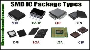
What is Chip Packaging?
Chip packaging is the process of enclosing an integrated circuit (IC) in a protective housing that allows it to communicate with other components on a circuit board. Essentially, it transforms a fragile silicon die into a usable component ready for mass production. The package protects the chip from physical damage, moisture, and environmental factors while providing electrical connections to the outside world.
Importance of IC Packaging
Integrated circuit packaging is more than just a protective shell. It affects the chip’s performance, reliability, and lifespan. For example, in consumer electronics, thin plastic packages provide low-cost protection and easy manufacturing. In high-performance servers or gaming GPUs, advanced packages like flip-chip ball grid arrays (BGA) enhance heat dissipation and signal integrity, allowing the chip to operate at higher speeds without overheating.
Key Components of a Semiconductor Package
Every chip package typically includes:
- Die: The actual silicon chip containing circuits.
- Lead frame or substrate: Conductive pathways that connect the die to the outside world.
- Encapsulation material: Plastic, ceramic, or metal that protects the die.
- Terminals or balls: Contact points that allow the package to connect to a PCB.
Types of Chip Packaging
Chip packaging comes in various types, each designed to meet specific requirements such as size, cost, thermal performance, and ease of manufacturing. Here are the most common types:
Through-Hole Packages
Through-hole packages are one of the oldest types of IC packaging. The chip’s leads pass through holes on the PCB and are soldered on the opposite side. While this method provides strong mechanical connections, it is less suited for high-density or high-speed circuits. Through-hole components are still widely used in power electronics, industrial machines, and hobbyist electronics.
Surface-Mount Packages (SMT)
Surface-mount technology revolutionized chip packaging by allowing components to be placed directly onto the surface of a PCB. SMT packages are smaller, lighter, and enable automated assembly. Common examples include small-outline integrated circuits (SOIC) and quad flat packages (QFP). These packages dominate consumer electronics because they allow higher component density and faster production.
Ball Grid Array (BGA) and Chip-Scale Packages (CSP)
BGA packages use an array of solder balls on the bottom of the package for connection to the PCB. This design improves thermal performance and signal integrity compared to traditional leaded packages. Chip-scale packages are even smaller, nearly the same size as the silicon die itself, making them ideal for smartphones, tablets, and wearables. Both types require precise manufacturing and soldering techniques but offer superior performance in high-speed applications.
Advanced Packaging Technologies
Modern electronics demand more from chip packaging than ever before. Advanced packaging includes multi-chip modules (MCM), 3D stacking, and heterogeneous integration, where multiple chips or components are combined in a single package. These innovations enable faster data processing, reduce power consumption, and allow for thinner, lighter devices. Industry leaders like Intel, TSMC, and AMD are investing heavily in these technologies to keep up with the growing demand for high-performance computing.
Chip Packaging Materials
The choice of packaging material affects cost, thermal performance, and mechanical strength. Engineers select materials based on the application, operating environment, and performance requirements.
Plastic Packages
Plastic encapsulation is the most common and cost-effective method. It provides adequate protection for consumer electronics while allowing automated manufacturing. However, plastic has lower thermal conductivity, so designers must manage heat through the PCB or additional cooling methods.
Ceramic Packages
Ceramic packages offer excellent thermal performance and mechanical strength, making them suitable for high-reliability applications such as aerospace, automotive, and military electronics. They can withstand high temperatures and provide a hermetic seal to protect sensitive circuits from moisture and contamination.
Metal and Hybrid Packages
Metal or metal-ceramic hybrid packages are used in high-power electronics. Metals provide superior heat dissipation, electrical shielding, and structural integrity. These packages are common in power transistors, RF components, and high-performance microprocessors.
Chip Packaging Processes
Transforming a silicon die into a fully packaged chip requires several precise steps. Each stage is critical to ensure reliability and performance.
Die Attachment
The first step is securing the silicon die to the lead frame or substrate. This can be done using conductive adhesives, solder, or epoxy. Proper attachment ensures thermal and electrical conductivity while preventing physical movement of the die.
Wire Bonding
Wire bonding connects the die’s pads to the package leads. Thin gold or aluminum wires are typically used. This step is delicate, as improper bonding can lead to electrical failure. In flip-chip packages, solder bumps replace wire bonds for direct connections.
Encapsulation
Encapsulation protects the die and wiring from mechanical damage and environmental factors. Materials like epoxy, ceramic, or metal are molded around the die. For high-reliability applications, hermetic sealing is used to prevent moisture ingress.
Testing and Quality Control
After packaging, chips undergo rigorous testing, including electrical tests, thermal cycling, and mechanical stress tests. Only components that meet specifications are shipped for assembly. Quality control is essential, as even minor defects can lead to catastrophic failures in critical systems.
Applications and Trends
Chip packaging is not just about protecting silicon; it drives innovation across industries. The choice of package impacts performance, size, and reliability.
Packaging in Consumer Electronics
For smartphones, tablets, and laptops, small, lightweight packages are preferred. CSPs and BGAs allow manufacturers to fit more functionality into a smaller footprint. Proper packaging ensures heat management, extending device lifespan and performance.
Packaging in High-Performance Computing
Servers, GPUs, and data centers demand chips that handle high power and fast signal transmission. Advanced packages, including 3D stacking and multi-chip modules, improve thermal performance and reduce latency. These packages are critical for AI workloads, scientific computing, and gaming performance.
Emerging Technologies (3D Packaging and Heterogeneous Integration)
3D packaging and heterogeneous integration are revolutionizing the semiconductor industry. In 3D packaging, multiple dies are stacked vertically within a single package, reducing the distance for electrical signals and improving performance. Heterogeneous integration combines different types of chips: such as logic, memory, and sensors into one package. These innovations enable smaller, faster, and more energy-efficient devices, crucial for AI, IoT, and mobile applications.
Challenges in Chip Packaging
Despite advancements, chip packaging faces several challenges that engineers must overcome to maintain performance and reliability.
Heat Dissipation
As chips become smaller and more powerful, heat management becomes critical. Overheating can degrade performance and shorten the chip’s lifespan. Engineers address this through thermal materials, heat sinks, and advanced packaging designs such as BGA or metal-backed packages.
Miniaturization Limitations
While consumers demand smaller devices, miniaturizing chip packages presents physical and manufacturing challenges. Smaller packages make assembly and testing more difficult, increasing the risk of defects. Advanced lithography and precision manufacturing techniques help overcome these limitations.
Cost vs. Performance Trade-offs
High-performance packaging technologies are often expensive. Companies must balance cost, performance, and reliability. For consumer electronics, low-cost plastic packages may suffice, while aerospace or high-performance computing demands premium ceramic or metal packages.
Helpful Tips for Understanding Chip Packaging
- Always consider the application: Mobile devices need small, lightweight packages, while servers prioritize thermal performance.
- Understand the basic types first: Through-hole, SMT, BGA, and CSP cover most common scenarios.
- Check manufacturer datasheets: They provide package dimensions, thermal limits, and recommended PCB layouts.
- Remember that advanced packaging can significantly impact power consumption and signal integrity.
Featured Snippet Section: FAQs About Chip Packaging
1. What is chip packaging?
Chip packaging is the process of enclosing a semiconductor die in a protective housing that allows it to connect to a circuit board and operate reliably.
2. Why is chip packaging important?
It protects the chip from damage, ensures proper electrical connections, manages heat, and allows for easy integration into electronic devices.
3. What are the main types of chip packaging?
The main types are through-hole packages, surface-mount packages (SMT), ball grid arrays (BGA), and chip-scale packages (CSP), each suited for different applications.
4. What materials are used in chip packaging?
Common materials include plastic, ceramic, metal, and hybrid combinations. The choice depends on thermal performance, mechanical strength, and cost requirements.
5. What is advanced chip packaging?
Advanced packaging includes 3D stacking, multi-chip modules (MCM), and heterogeneous integration, which improve performance, reduce size, and enhance energy efficiency.
6. How does chip packaging affect performance?
Packaging influences thermal management, signal integrity, electrical connectivity, and reliability. A well-designed package improves overall chip efficiency and lifespan.
7. Can chip packaging be customized?
Yes, manufacturers can design custom packages to meet specific electrical, thermal, or mechanical requirements, especially for specialized applications like aerospace or high-performance computing.
Step-by-Step Guide to Selecting Chip Packaging
- Identify the application requirements: Determine size, power, thermal, and signal needs.
- Choose the package type: Select through-hole, SMT, BGA, CSP, or advanced packages.
- Select appropriate materials: Plastic for cost-effective solutions, ceramic or metal for high reliability.
- Consider manufacturing capabilities: Ensure your assembly process supports the chosen package.
- Test and validate: Perform thermal, electrical, and mechanical tests before production.
Comparing Popular Chip Packages
| Package Type | Size | Cost | Performance | Typical Use |
|---|---|---|---|---|
| Through-Hole | Large | Low | Moderate | Power electronics, industrial machines |
| Surface-Mount (SMT) | Small | Moderate | Good | Consumer electronics, laptops |
| Ball Grid Array (BGA) | Medium | High | Excellent | High-performance GPUs, servers |
| Chip-Scale Package (CSP) | Very Small | High | Excellent | Smartphones, tablets, wearables |
Final Thoughts
Understanding chip packaging is essential for anyone interested in electronics, engineering, or technology. From the humble through-hole component to advanced 3D stacked modules, packaging plays a critical role in performance, reliability, and innovation. Whether you are a hobbyist designing circuits at home or an engineer developing cutting-edge processors, knowing the right packaging strategy can make all the difference. By considering application requirements, materials, and manufacturing processes, you can ensure that your chips not only survive but thrive in the devices they power.